Product Information
Copper-based PCB or copper core PCB is a metal core PCB using copper as the base material. Like all metal core PCBs, it also has three main layers. The top layer is made of copper, which is responsible for the electrical connection between the components. This layer is standard in all types of PCBs. The second layer is the dielectric layer that prevents current from the top layer to the base layer. Although this layer is electrically an insulator, it is a good conductor of heat. It transfers the heat produced by the components and helps in heat dissipation. The bottom layer of the PCB is copper, which is why it is a copper core PCB.Copper-based PCB provide the best performance among all-metal core PCBs. These PCBs are used for particular purposes, including high-frequency circuits and high-temperature variations. They can dissipate heat better than iron and aluminum core PCBs.
Applications for Copper-based PCB
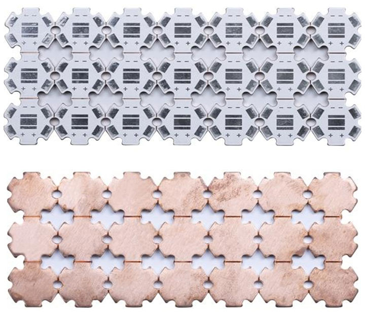
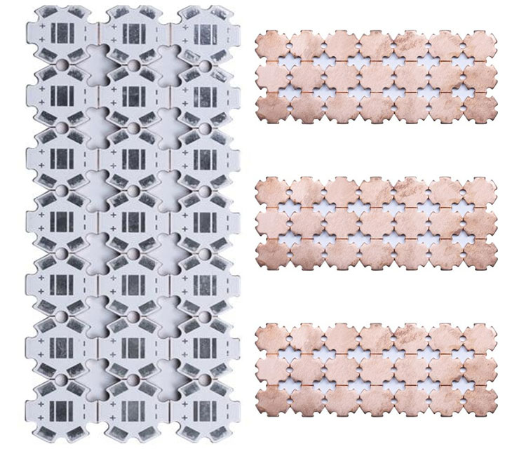
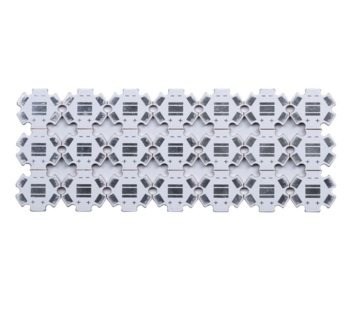
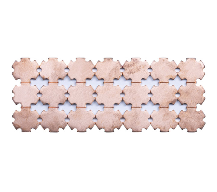
5050 copper substrate is a commonly used substrate, mainly used in electronic products, LED lighting and industrial electronic control. Customized 5050 copper substrate processing can enable customers with different needs to obtain copper substrates that precisely meet the requirements. The processing of customized copper substrates can meet the requirements of different specifications such as different sizes, shapes, and thicknesses, so that it can be widely used in different industries.
The Necessity of Using Copper-based PCB
Copper substrate is the most expensive kind of metal substrate, and its thermal conductivity is many times better than that of aluminum substrate and iron substrate. It is suitable for high-frequency circuits and areas with large changes in high and low temperature, as well as heat dissipation of precision communication equipment and architectural decoration industries.
Copper substrates are divided into immersion gold copper substrates, silver-plated copper substrates, tin-sprayed copper substrates, anti-oxidation copper substrates, etc.
The copper substrate circuit layer is required to have a large current-carrying capacity, so thicker copper foil should be used, and the thickness is generally 35 μm to 280 μm;
The thermally conductive insulating layer is the core technology of the copper substrate. The core thermally conductive component is composed of aluminum oxide and silicon powder and a polymer filled with epoxy resin. It has small thermal resistance (0.15), excellent viscoelastic performance, and has the ability to resist thermal aging. Ability to withstand mechanical and thermal stress.
The metal base layer is the supporting member of the copper substrate, which requires high thermal conductivity. It is generally a copper plate, which is suitable for conventional machining such as drilling, punching and cutting.
The basic production process of Copper Substrate PCB :
- Cutting: Cut the copper substrate raw material into the size required for production.
- Drilling: Carry out positioning drilling on the copper substrate to provide assistance for subsequent processing.
- Circuit imaging: present the required part of the circuit on the copper substrate sheet.
- Etching: keep the required part after the circuit imaging. The rest do not need to be partially etched away.
- Silk screen solder resistance: prevent non-soldering points from being contaminated with solder, and prevent tin from entering and causing short circuits. The solder mask is particularly important when performing wave soldering, which can effectively protect the circuit from moisture.
- Silk screen characters: for marking.
- Surface treatment: to protect the surface of the copper substrate.
- CNC: Perform CNC operations on the entire board.
- Withstanding voltage test: test whether the circuit works normally.
- Packaging and shipment: The copper substrate confirms that the packaging is complete and beautiful, and the quantity is correct.
Why Choose HSX
Top Cooper base material resources, so that your products win at the root
With the continuous development and progress of science and technology, the application field of 5050 copper substrate is also expanding. Copper substrates can play an important role in different industries. In the electronic product manufacturing industry, copper substrates are the main circuit boards, and customized processing can better meet the different needs of various electronic products for copper substrates. In LED outdoor lighting, the demand has also increased in the past two years.
The process of processing and customizing copper substrates requires more processes and is technically difficult, so the price and time are more expensive and longer than aluminum substrates. Correctly select the processing method and adjust the processing parameters during the processing to avoid adverse phenomena in the processing. At the same time, after the processing is completed, strict inspection and testing work is required to ensure that the copper substrate is of good quality and meet the requirements and expectations of customers. .
5050 copper substrate processing customization can meet the various requirements of different industries, meet the different needs of customers for copper substrates, improve the efficiency and quality of material use, and also promote the progress and development of the industry. In the future, with the continuous improvement of people’s requirements for materials and further technological innovation, the market prospect of customized copper substrate processing will be broader.
Copper substrate PCB processing, LED copper substrate thermal conductivity parameters
When processing copper substrates in circuit board factories, attention should be paid to the thermal conductivity requirements of copper substrates provided by customers. The thermal conductivity is an important parameter for the heat dissipation performance of copper-based circuit boards, and it is also one of the standards for measuring the quality of LED copper substrates. The other two are thermal conductivity. resistance and withstand voltage. Usually the so-called heat conduction principle is the efficiency of heat conduction at the graphic level of the copper-based PCB board to transfer heat to the substrate through the heat-conducting insulating layer.
The following are the detailed parameters of copper-based circuit boards:
a. diamond 1300-2400, b. silicon 611, c. silver 429, d. copper 401, e. gold 317, f. beryllium 250, g. aluminum 240, h. aluminum nitride 200, i. tungsten 180, j . Zinc 116, k. Nickel 91, l. Iron 84-90
Among them, since the heat dissipation performance of the copper substrate is essentially better than that of the aluminum substrate and the iron substrate, the heat dissipation performance of the copper substrate is one of the standards for measuring the quality of the board, and it is also the most popular substrate used in the industry. The thermal conductivity of the copper substrate can be obtained by testing the test equipment after the plates are pressed together. The highest thermal conductivity value is generally ceramics. However, due to cost considerations, most of the current market is copper substrates, aluminum substrates, and copper substrates. The heat dissipation performance is faster than the aluminum substrate.
The thermal conductivity of the relative copper substrate is a parameter that everyone cares about. It is divided into thermoelectric separation copper substrate and ordinary copper substrate. The thermal conductivity of thermoelectric separation copper substrate is 398W, while the thermal conductivity of ordinary copper substrate is 1W 2W 3W….8W . The higher the thermal conductivity, the better the performance. Copper substrate is a unique metal-based copper-clad laminate substrate, which has good thermal conductivity, electrical insulation performance, and heat dissipation performance. It is generally used in new energy vehicle lighting electronics, LED high-power lighting, medical optical instruments, communication base station equipment, digital Electronic products such as projectors.
Copper substrate PCB processing, LED copper substrate thermal conductivity parameters
When processing copper substrates in circuit board factories, attention should be paid to the thermal conductivity requirements of copper substrates provided by customers. The thermal conductivity is an important parameter for the heat dissipation performance of copper-based circuit boards, and it is also one of the standards for measuring the quality of LED copper substrates. The other two are thermal conductivity. resistance and withstand voltage. Usually the so-called heat conduction principle is the efficiency of heat conduction at the graphic level of the copper-based PCB board to transfer heat to the substrate through the heat-conducting insulating layer.
The following are the detailed parameters of copper-based circuit boards:
a. diamond 1300-2400, b. silicon 611, c. silver 429, d. copper 401, e. gold 317, f. beryllium 250, g. aluminum 240, h. aluminum nitride 200, i. tungsten 180, j . Zinc 116, k. Nickel 91, l. Iron 84-90
Among them, since the heat dissipation performance of the copper substrate is essentially better than that of the aluminum substrate and the iron substrate, the heat dissipation performance of the copper substrate is one of the standards for measuring the quality of the board, and it is also the most popular substrate used in the industry. The thermal conductivity of the copper substrate can be obtained by testing the test equipment after the plates are pressed together. The highest thermal conductivity value is generally ceramics. However, due to cost considerations, most of the current market is copper substrates, aluminum substrates, and copper substrates. The heat dissipation performance is faster than the aluminum substrate.
PCB acceptance criteria
- IPC-A-600G standard (PCB conformity standard);
- GJB326A-96(military standard);
- IPC-6018A (high frequency board acceptance standards)
- Implementation of quality PDCA cycle process, continuous improvement of product performance imported from the United States Diane ion chromatography tester (DIONEXICS-900) and temperature cycle inspection equipment to ensure high reliability and stability of the product.
Why Choose HSX
Top high-frequency material resources, so that your products win at the root
The factory always has imported and domestic plates with dielectric constants ranging from 2.2 to 10.6
- High frequency materials: Rogers/Rogers, taconic/taikangli, Arlon, Isola, F4BM/Wangling, PTFE/Teflon, TP-2, etc., with dielectric constants ranging from 2.2 to 10.6.
- Rogers series: Rogers RO4350B, RO4003C, RT5880, RT5870, ro3003, ro3010, RO4730, RT6006, RT6010, etc.
Leading process capability to meet high frequency PCB manufacturing needs
- Max. thickness to diameter ratio 10:1 Max. copper thickness 6OZ Max. working board size 2000x610mm
- The thinnest 4-layer board 0.33mm The smallest hole 0.10mm
- Minimum line width/line spacing 3mil/3mil
- Proven hybrid technology: ROGERS/Rogers+FR4,FR4+PTFE,FR4+408HR,ceramic+FR4 etc.
Experienced
PCB high-frequency board samples + small and medium batch, more than ten years of experience, skilled in PCB high-frequency board expertise
Products are: FR4 glass fiber board double-sided multilayer circuit board / high frequency board / high frequency circuit board / high frequency mixed laminate / mixed media laminate / F4B high frequency board / microwave RF board / high frequency microwave board, etc., the power splitter, coupler, combiner, power amplifier, dry amplifier, base station, RF antenna, 4G antenna used in the high frequency circuit board has professional production experience
PCB acceptance criteria
- IPC-A-600G standard (PCB conformity standard);
- GJB326A-96(military standard);
- IPC-6018A (high frequency board acceptance standards)
- Implementation of quality PDCA cycle process, continuous improvement of product performance imported from the United States Diane ion chromatography tester (DIONEXICS-900) and temperature cycle inspection equipment to ensure high reliability and stability of the product.


