Product Information
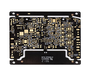
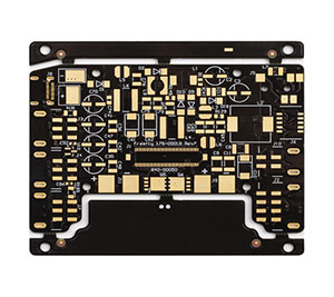
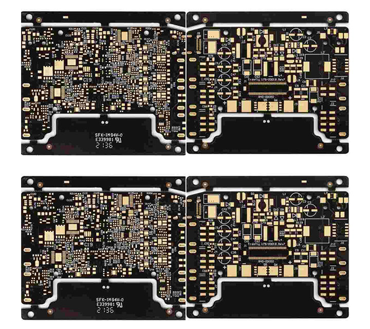
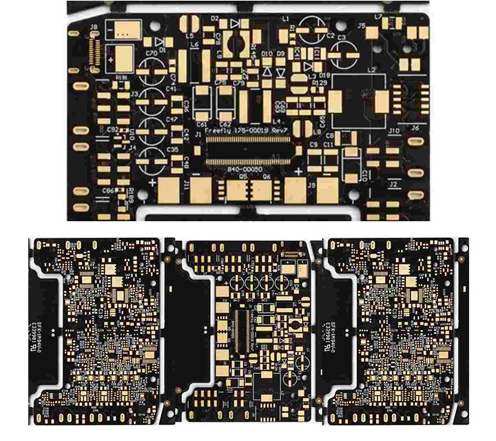
- What’s HDI PCB? High-density interconnect (HDI) PCBs are characterized by finer lines, closer spaces, and more dense wiring, which allow for a faster connection while reducing the size and bulk of a project. These boards also feature blind and buried vias, laser ablatedmicrovias, sequential lamination, and via in-pads.
As a result, a HDI board can house the functionality of the previous boards used. MADPCB is an HDI PCB manufacturer and provider in Shenzhen, China supports HDI PCB prototype and mass production with less expensive price and quick-turn lead time. Customers from a variety of industries we serve have a common that have high expectations in quality, reliability and on-time delivery in HDI PCB production. Our quality is not afterthought, but built into each process from front-end to fabrication and shipping.
Applications for HDI PCB
HDI stands for High-Density Interconnector. It is a special type of PCB that has the capability of high-density interconnections. It means that HDI boards has more wires or conduction lines per unit area, utilizing the most out of the space and offering a compact PCB.
HDI PCB has tightly packed interconnections, it saves a lot of space and offers more component density and it has the capability of making a circuit compact.
HDI boards are particularly attractive to portable, mobile, and portable electronics due to their slim, dependable performance and tiny size. HDI technology is a critical component of many of advanced technologies. The miniaturization of electronic components including PCBs has enabled manufacturers to produce smaller, more cost-effective devices without sacrificing performance or reliability.
They are largely used in Consumer Electronics, communication, Automotive and Aerospace,Medical Devices, and industry control products and other industries.
What is HDI PCB?
HDI PCB means high density interconnect printed circuit boards, they are characterized by finer lines, closer spaces, and more dense wiring.
Due to its higher circuit density than traditional circuit boards, HDI PCB designs can include smaller through holes and capture pads, as well as higher connection pad density. HDI PCB is widely used to reduce the weight and overall dimensions of products, as well as to enhance the electrical performance of the device.
- HDI Board Stack-up:
1+N+1 with laser microvia and mechanical buried core via. The “1” represents “build-up” or sequential lamination on each side of the core.
i+N+i (i>=2) PCBs contain 2 or more “build-up” of high-density interconnect layers. Microvias on different layers can be staggered or stacked. Copper filled stacked microvia structures are commonly seen in challenging designs.
HSX products cover 1~32L FR-4 PCB, IMS PCB,HDI Boards, high frequency PTFE boards and Rigid-flex boards etc. It provides flexible quick turn production services (12 hours to72 hours), as well as small volume to big volume PCB manufacturing.Products are widely used in high-tech fields such as communications, power supplies, computer networks, digital products, industrial control, science and education, medical devices, and aerospace.
Why Choose HSX
Top high-frequency material resources, so that your products win at the root
The factory always has imported and domestic plates with dielectric constants ranging from 2.2 to 10.6
- High frequency materials: Rogers/Rogers, taconic/taikangli, Arlon, Isola, F4BM/Wangling, PTFE/Teflon, TP-2, etc., with dielectric constants ranging from 2.2 to 10.6.
- Rogers series: Rogers RO4350B, RO4003C, RT5880, RT5870, ro3003, ro3010, RO4730, RT6006, RT6010, etc.
Leading process capability to meet high frequency PCB manufacturing needs
- Max. thickness to diameter ratio 10:1 Max. copper thickness 6OZ Max. working board size 2000x610mm
- The thinnest 4-layer board 0.33mm The smallest hole 0.10mm
- Minimum line width/line spacing 3mil/3mil
- Proven hybrid technology: ROGERS/Rogers+FR4,FR4+PTFE,FR4+408HR,ceramic+FR4 etc.
Experienced
- PCB high-frequency board samples + small and medium batch, more than ten years of experience, skilled in PCB high-frequency board expertise
- Products are: FR4 glass fiber board double-sided multilayer circuit board / high frequency board / high frequency circuit board / high frequency mixed laminate / mixed media laminate / F4B high frequency board / microwave RF board / high frequency microwave board, etc., the power splitter, coupler, combiner, power amplifier, dry amplifier, base station, RF antenna, 4G antenna used in the high frequency circuit board has professional production experience
PCB acceptance criteria
- IPC-A-600G standard (PCB conformity standard);
- GJB326A-96(military standard);
- IPC-6018A (high frequency board acceptance standards)
- Implementation of quality PDCA cycle process, continuous improvement of product performance imported from the United States Diane ion chromatography tester (DIONEXICS-900) and temperature cycle inspection equipment to ensure high reliability and stability of the product.
Why Choose HSX
Top high-frequency material resources, so that your products win at the root
The factory always has imported and domestic plates with dielectric constants ranging from 2.2 to 10.6
- High frequency materials: Rogers/Rogers, taconic/taikangli, Arlon, Isola, F4BM/Wangling, PTFE/Teflon, TP-2, etc., with dielectric constants ranging from 2.2 to 10.6.
- Rogers series: Rogers RO4350B, RO4003C, RT5880, RT5870, ro3003, ro3010, RO4730, RT6006, RT6010, etc.
Leading process capability to meet high frequency PCB manufacturing needs
- Max. thickness to diameter ratio 10:1 Max. copper thickness 6OZ Max. working board size 2000x610mm
- The thinnest 4-layer board 0.33mm The smallest hole 0.10mm
- Minimum line width/line spacing 3mil/3mil
- Proven hybrid technology: ROGERS/Rogers+FR4,FR4+PTFE,FR4+408HR,ceramic+FR4 etc.
Experienced
PCB high-frequency board samples + small and medium batch, more than ten years of experience, skilled in PCB high-frequency board expertise
Products are: FR4 glass fiber board double-sided multilayer circuit board / high frequency board / high frequency circuit board / high frequency mixed laminate / mixed media laminate / F4B high frequency board / microwave RF board / high frequency microwave board, etc., the power splitter, coupler, combiner, power amplifier, dry amplifier, base station, RF antenna, 4G antenna used in the high frequency circuit board has professional production experience
PCB acceptance criteria
- IPC-A-600G standard (PCB conformity standard);
- GJB326A-96(military standard);
- IPC-6018A (high frequency board acceptance standards)
- Implementation of quality PDCA cycle process, continuous improvement of product performance imported from the United States Diane ion chromatography tester (DIONEXICS-900) and temperature cycle inspection equipment to ensure high reliability and stability of the product.
