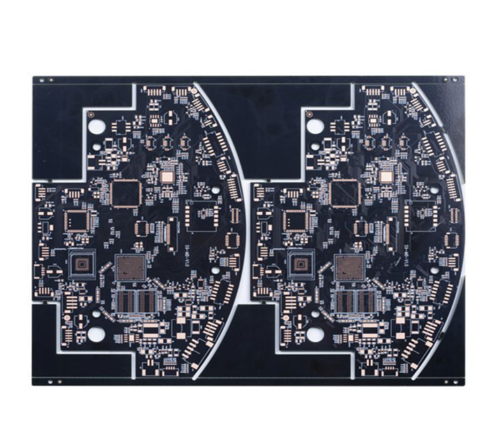
Product Information
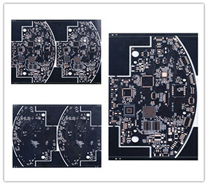
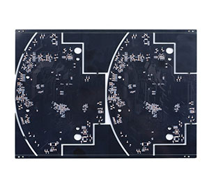
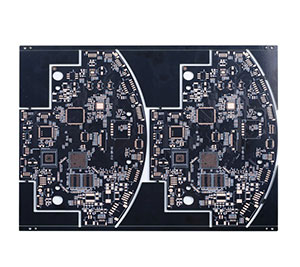
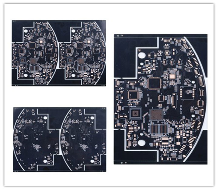
Multilayer PCB
PCB multilayer boards refer to multilayer circuit boards used in electrical products, which use more single or double sided wiring boards. A printed circuit board that uses one double-sided inner layer, two single-sided outer layers, or two double-sided inner layers, and two single-sided outer layers, and is interconnected with conductive patterns according to design requirements through positioning systems and insulating bonding materials, becomes a four-layer or six-layer printed circuit board, also known as a multi-layer printed circuit board. The structure is as follows:
The Structure of Multilayer PCB
The Structure of Multilayer PCB is as follows:
- Signal layer
AlTIum Designer can provide up to 32 signal layers, including the top layer, bottom layer, and middle layer. Each layer can be interconnected through through-holes, blind holes, and buried holes.
(1) Top signal layer
Also known as component layer, it is mainly used to place components. For double-layer and multi-layer boards, it can be used to arrange wires or copper clad.
(2) Bottom signal layer
Also known as a welding layer, it is mainly used for wiring and welding, and can be used to place components on double-layer and multi-layer boards.
(3) Intermediate signal layer
There can be up to 30 layers, which are used to arrange signal lines in a multi-layer board, excluding power lines and ground wires.
- Internal power supply layer
Generally referred to as the internal electrical layer, it only occurs in multilayer boards. The number of PCB layers generally refers to the sum of the signal layer and the internal electrical layer. Similar to the signal layer, the internal electrical layer and the internal electrical layer, as well as the internal electrical layer and the signal layer, can be interconnected through t
The Application of Multilayer PCB
As a version based on traditional circuit boards for processing and upgrading, multi-layer PCB circuit boards are only in their infancy when they are put into the market. The following is a brief introduction to consumers of the current application fields of multilayer PCB circuit boards.
1. Printing industry
2. The field of electronic equipment
3. Smart home layout field
Why are multilayer PCB circuit boards becoming more and more popular
1. Simple structure
In order to meet the isolation between channels, the multi-layer PCB circuit board structure adopts a frame-type metal material isolation cavity. The whole module is divided into multiple independent small cavities, and the circuit unit in each small cavity forms a relatively independent part. At the position of the microstrip line at the connection of the circuit unit, the isolation strip is hollowed out to prevent short circuit. Other parts are in contact with the top substrate in a large area to achieve isolation and good grounding between channels. When assembling, the printed board is embedded into the cavity from the bottom of the cavity and fastened with screws to form a structure similar to a sandwich biscuit.
2. Automatic adjustment
The core of PCB component layout is to arrange the signal link microwave components reasonably. By adjusting the direction and position of the components, the length of the signal transmission path is small and the input is far away from the output. At the same time, high-power circuits and low-power circuits are kept away from each other, and sensitive analog signals are kept away from high-speed digital signals and microwave radio frequency signals. In the design, the decoupling capacitors are directly connected to the chip pins through wires. The decoupling capacitor should be as close as possible to the power pin of the chip, and the self-resonant frequency of the selected decoupling capacitor includes the noise frequency, so that the filtering effect of the power supply entering the chip can be better.
3. Safe and reliable
More current-type driver chips are used in the circuit board. When the circuit is running, when multiple devices switch simultaneously, a large transient current will pass through the chip and the power plane of the circuit board. At this time, the large The current surge will cause the ground plane voltage to fluctuate, thereby avoiding interference to other static drivers and microwave chips of the same power supply, so it is safer and more reliable.
Why Choose HSX
Top high-frequency material resources, so that your products win at the root
The factory always has imported and domestic plates with dielectric constants ranging from 2.2 to 10.6
- High frequency materials: Rogers/Rogers, taconic/taikangli, Arlon, Isola, F4BM/Wangling, PTFE/Teflon, TP-2, etc., with dielectric constants ranging from 2.2 to 10.6.
- Rogers series: Rogers RO4350B, RO4003C, RT5880, RT5870, ro3003, ro3010, RO4730, RT6006, RT6010, etc.
Leading process capability to meet high frequency PCB manufacturing needs
- Max. thickness to diameter ratio 10:1 Max. copper thickness 6OZ Max. working board size 2000x610mm
- The thinnest 4-layer board 0.33mm The smallest hole 0.10mm
- Minimum line width/line spacing 3mil/3mil
- Proven hybrid technology: ROGERS/Rogers+FR4,FR4+PTFE,FR4+408HR,ceramic+FR4 etc.
Experienced
- PCB high-frequency board samples + small and medium batch, more than ten years of experience, skilled in PCB high-frequency board expertise
- Products are: FR4 glass fiber board double-sided multilayer circuit board / high frequency board / high frequency circuit board / high frequency mixed laminate / mixed media laminate / F4B high frequency board / microwave RF board / high frequency microwave board, etc., the power splitter, coupler, combiner, power amplifier, dry amplifier, base station, RF antenna, 4G antenna used in the high frequency circuit board has professional production experience
PCB acceptance criteria
- IPC-A-600G standard (PCB conformity standard);
- GJB326A-96(military standard);
- IPC-6018A (high frequency board acceptance standards)
- Implementation of quality PDCA cycle process, continuous improvement of product performance imported from the United States Diane ion chromatography tester (DIONEXICS-900) and temperature cycle inspection equipment to ensure high reliability and stability of the product.
Why Choose HSX
Top high-frequency material resources, so that your products win at the root
The factory always has imported and domestic plates with dielectric constants ranging from 2.2 to 10.6
- High frequency materials: Rogers/Rogers, taconic/taikangli, Arlon, Isola, F4BM/Wangling, PTFE/Teflon, TP-2, etc., with dielectric constants ranging from 2.2 to 10.6.
- Rogers series: Rogers RO4350B, RO4003C, RT5880, RT5870, ro3003, ro3010, RO4730, RT6006, RT6010, etc.
Leading process capability to meet high frequency PCB manufacturing needs
- Max. thickness to diameter ratio 10:1 Max. copper thickness 6OZ Max. working board size 2000x610mm
- The thinnest 4-layer board 0.33mm The smallest hole 0.10mm
- Minimum line width/line spacing 3mil/3mil
- Proven hybrid technology: ROGERS/Rogers+FR4,FR4+PTFE,FR4+408HR,ceramic+FR4 etc.
Experienced
PCB high-frequency board samples + small and medium batch, more than ten years of experience, skilled in PCB high-frequency board expertise
Products are: FR4 glass fiber board double-sided multilayer circuit board / high frequency board / high frequency circuit board / high frequency mixed laminate / mixed media laminate / F4B high frequency board / microwave RF board / high frequency microwave board, etc., the power splitter, coupler, combiner, power amplifier, dry amplifier, base station, RF antenna, 4G antenna used in the high frequency circuit board has professional production experience
PCB acceptance criteria
- IPC-A-600G standard (PCB conformity standard);
- GJB326A-96(military standard);
- IPC-6018A (high frequency board acceptance standards)
- Implementation of quality PDCA cycle process, continuous improvement of product performance imported from the United States Diane ion chromatography tester (DIONEXICS-900) and temperature cycle inspection equipment to ensure high reliability and stability of the product.
